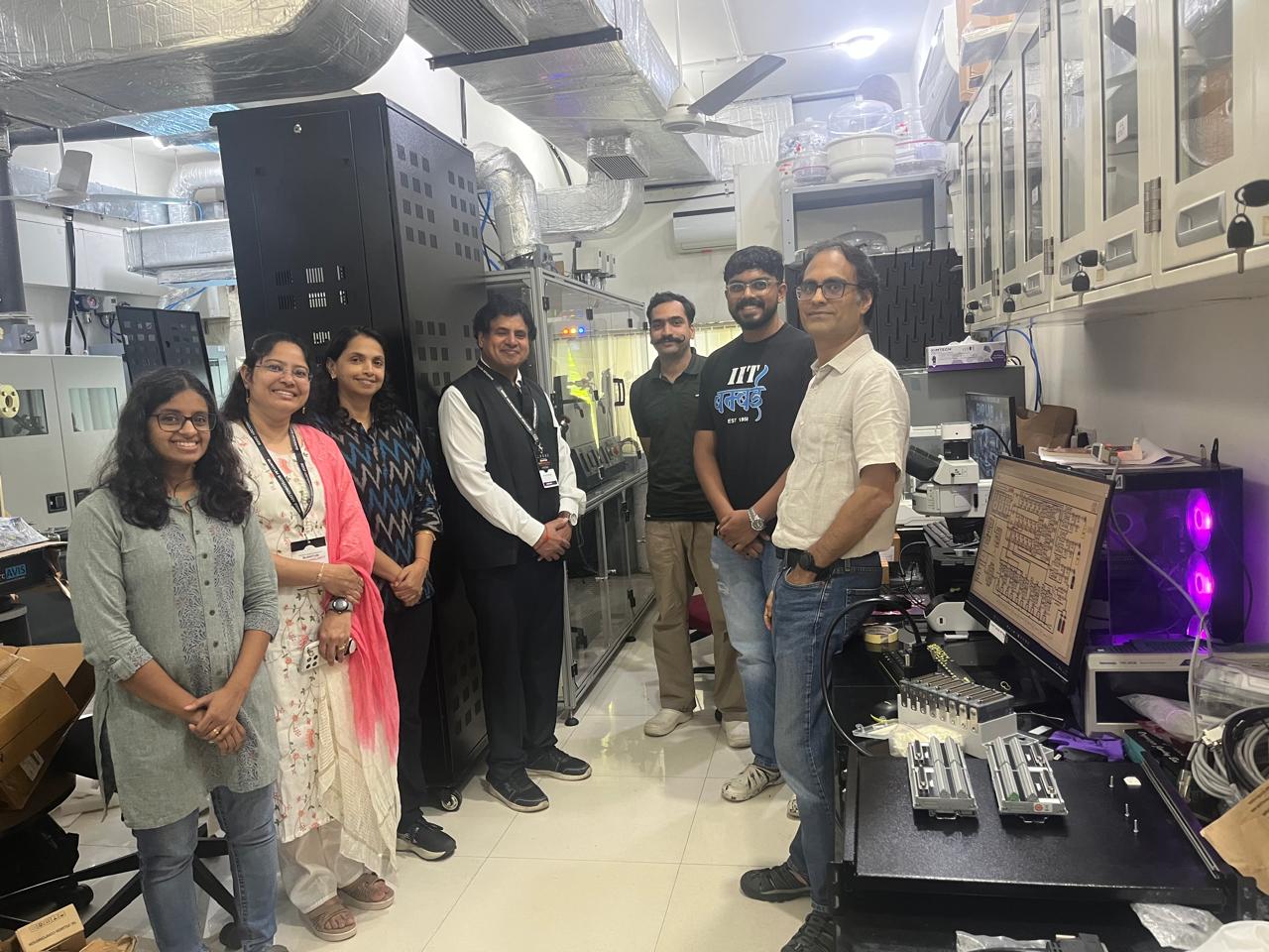
Electronic Material Processing (EMP): Layered Semiconductor Lab, IIT Bombay
The EMP Lab is dedicated to advancing scalable synthesis and defect engineering of 2D layered materials, with a particular focus on wafer-scale TMDC growth, understanding growth mechanisms, and tailoring material properties for optoelectronic applications.
The group also develops advanced research instrumentation in-house, including building MOCVD and inductively coupled plasma (ICP) systems from the ground up, enabling greater flexibility and control over materials synthesis and processing.
Team Members
Prof. Tanushree Choudhury (MPI)

Assistant Professor
Department of Metallurgy & Material Science
Indian Institute of Technology Bombay
Email: tanuhc@iitb.ac.in
Diwakar Singh
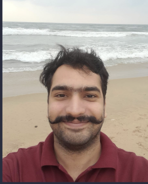
PhD Candidate
Department of MEMS
Indian Institute of Technology Bombay
Email: diwakar.singh@iitb.ac.in
Supervisor: Prof. Tanushree H Choudhury
Linkedin: www.linkedin.com/in/diwakar-singh-006478167
Webpage: https://sites.google.com/view/singhdiwakar/home
Research Interest: Working on in-situ doping and wafer-scale growth of TMDs (MoS2, WS2, Mox W1-xS2), bridging experiments with COMSOL-based simulations, and evaluating thermal, optical, and electrical properties of these films.
Research Interests:
· 2D Materials
· Chemical Vapor Deposition
· Transition Metal Dichalcogenides
· CFD using COMSOL Multiphysics
Gayatri Subbulaxmi

PhD scholar
Department of MEMS
Indian Institute of Technology Bombay
Email: subhalaxmigayatri108@gmail.com
Supervisor: Prof. Tanushree H Choudhury
Linkedin: https://www.linkedin.com/in/gayatri-subhalaxmi
Webpage: https://share.google/ohhRR7JHbzFMOHoeu
Research Interest:
2D TMDC growth & defect engineering; optoelectronic and excitonic properties of TMDCs; Raman/PL spectroscopy and nanoscale optical characterization & quantum nanophotonics; flexible & wearable electronics
Her research experience encompasses:
(i) Site-selective, lithography-free defect engineering in TMDCs for tailoring their optoelectronic and excitonic properties;
(ii) Self-assembled nanospheres and their structural-color-based optical imaging, supported by a theoretical framework for determining their structural arrangement;
(iii) Surface-energy tuning of self-assembled liquid metals and developing flexible, stretchable, and wearable electronics.
Her broader research philosophy is centered on controlling material properties at the atomic and nanoscale levels and translating fundamental scientific understanding into scalable technologies for real-world and industrial applications.
Dr. Ramesh Rajarapu
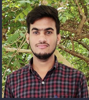
Postdoctoral Fellow
Department of MEMS
Indian Institute of Technology Bombay
Email: rajarapuramesh855@gmail.com
Supervisor: Prof. Tanushree H Choudhury
Linkedin: www.linkedin.com/in/rajarapu-ramesh-875b8b216
Google Scholar: https://scholar.google.com/citations?user=JpAH__gAAAAJ&hl=en
Webpage: https://sites.google.com/view/drrameshrajarapuphd/home
Research Interest: His research interests focus on the wafer scale synthesis and controlled doping of van der Waals materials (MoS2, WS2, MoO3, and VS2) by employing CVD/MOCVD processes for Quantum Optoelectronic Applications.
Research Interests:
Synthesis and Characterization of 2D Materia
Transition Metal Dichalcogenides and Their Properties
Multiphysics Modeling and CFD using COMSOL
Dr. Gaurav Bassi
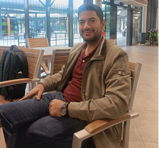
Postdoctoral Fellow
Department of MEMS
Indian Institute of Technology Bombay
Email: gaurav.bassi@iitb.ac.in
Supervisor: Prof. Tanushree H Choudhury
Linkedin: https://www.linkedin.com/in/gaurav-bassi-741557275/
Google scholar: https://scholar.google.com/citations?user=l8EPt-UAAAAJ&hl=en
PhD from IIT Ropar in June 2025
Research Interest: Working on wafer-scale growth of TMDs especially PtS2, PtSe2, MoS2, WS2, and its electrical and optoelectronics properties study.
Research Interests:
- 2D Materials
- Transition Metal Dichalcogenides (PtS2, PtSe2, MoS2, WS2)
- Chemical Vapor Deposition, Sputtering, thermal evaporator
- Photodetectors device fabrication and testing
Group Photo